Power BJT

Here present the article about the power BJT , and construction, structure, I-V characteristic and application.

➸Power BJT(Bipolar Junction Transistors)
  • Power transister are used to handle large current and large voltages.
  • the power handling capacity of the power transistors is very large.They have to dissipate a large power in the form of heat.
  • The size of power transistors is larger than that of the low power transistor.This is necessary for dissipating more power.
  • Sometimes power transistors are mounted on heatsinks. The heatsinks are made of metal and they increase the effective area of the power transistors.
  • The increased area allows easy transfer of heat to take place from the device to atmosphere.
 Construction of Power BJT:
  • The power bipolar junction transistor is supposed to block a high voltage in the off-state and have high current carrying capacity in the on-state.
  • In order to have these characteristics the power bipolar junction transistor(BJT)must have a very different structure than a small low power BJT.
  • Due to the modified structure the I-V characteristics and the switching behaviour of power BJT will be significantly different than its logical counterpart.
  • The base drive circuits will be different, and protection circuits will have to be included alongwith a power BJT.
Power BJT Structure:
  • A power transistor has a vertically oriented four-layer structure of alternating p-type and n-type layers with doping similar to the n-p-n transistor .
  • The power transistor has three terminals collector,base and emitter.
  • The n-p-n transistors are more widely used than the p-n-p transistors.
types of BJT :

There are two types of power BJT as shown in the figure above: 

1.NPN transistor :-

 the transistors in which base is positive and collector and emitter are both negative. NPN transistors are more commonly used and preffered over PNP transistors.
2.PNP transistor:
the transistors in which base is negative and collector and emitter are positive

Why is the vertical structure used?

  • The reason for using the vertical structure is that it increases the cross-sectional area through which the device current flows.
  • This will reduce the on-state resistance and hence the on-state power dissipation taking place in the transistor.
  • The vertical structure also minimizes the thermal resistance of the transistor(resistance offered to the flow of heat)and reduces the power dissipation.

I-V characteristic

The I-V characteristic of Power BJT divides into four regions.
  1. Cut-off region
  2. Active region
  3. Quasi-saturation region
  4. Hard saturation region


1. Cut-off region:

The BE and CB both junctions are reverse bias. The base current IB=0 and collector current IC is equal to the reverse leakage current ICEO. The region below the characteristic for IB=0 is cut-off region. In this region, BJT offers large resistance to the flow of current. Hence it is equivalent to an open circuit.

2. Active region:

The BE junction is forward bias and CB junction is reverse bias. The collector current IC increase slightly with an increase in the voltage VCE if IB is increased. The relation of IB and IC is, IC=βdcIB is true in the active region.
If BJT uses as an amplifier or as a series pass transistor in the voltage regulator, it operates in this region. The dynamic resistance in this region is large. The power dissipation is maximum.

3. Quasi-saturation region:

Quasi-saturation region is between the hard saturation and active region. This region exists due to the lightly doped drift layer. When the BJT operates at high frequency, it is operated in this region. Both junctions are forward bias. The device offers low resistance compared to the active region. So, power loss is less. In this region, the device does not go into deep saturation. So, it can turn off quickly. Therefore, we can use for higher frequency applications.

4. Hard-saturation region:

The Power BJT push into the hard-saturation region from the quasi-saturation region by increasing the base current. This region is also known as deep saturation region. The resistance offers in this region is minimum. It is even less than the quasi-saturation region. So, when the BJT operates in this region, power dissipation is minimum. The device acts as a closed switch when it operates in this region. But it needs more time to turn off. So, this region is suitable only for low-frequency switching application. In this region, both junctions are forward bias. The collector current is not proportional to the base current, IC remains almost constant at IC(sat) and independent from the value of base current.
Doping levels:


  •  the doping levels in each of the layers.The thickness of the different layers will have a significant effect on the characteristics of the device. 
  • the emitter layer is heavily doped.The base is moderately doped.The(n-)region is known as the collector drift region and it is lightly doped.
  • The(n+)region next to the drift region has doping level similar to that of emitter.This(n+)region serves the collector region.
  • The base region(p)is moderately doped and it is thin as compared to the drift region.

Applications of power BJT :

some of the typical application areas are:


  1. as series pass transister in regulated power supply
  2. the final audio amplifier in the stereo system
  3. power amplifiers 
  4. switched mode power supplies(SMPS)
  5. relay and display drivers
  6. AC motor speed controllers
  7. DC / AC Inverters.

You can also read this :
 ðŸ‘‡ 👇 👇 👇 👇👇 👇

https://electricalmafia.blogspot.com/2019/03/what-is-diode.html

https://electricalmafia.blogspot.com/2019/03/what-is-led.html

https://electricalmafia.blogspot.com/2019/03/how-is-principal-of-dc-generator.html

https://electricalmafia.blogspot.com/2019/03/marx-generator.html
What is LED?

Here present the LED. and this article to knowledge about LED.

LED is light emitting diode. LED are a simple invention with huge potential to change the lighting industry for the better.


What is LED?
A light emitting diode is a semiconductor device that emits visible light when an electrical current passes through it. It is essentially the opposite of a photovoltaic cell(a device that converts visible light into electrical current.)

 Light emitting PN-junction diode.
       – Visible or infrared light.
• Recall diodes act as a one way gate to       current flow.
– A forward-biased PN-junction diode     allows current flow from anode to cathode.
• An LED conducts and emits light when its anode is made more positive (approx. 
1.4V) than its cathode. 
– With reverse polarity, LED stops conducting and emitting light.

How LED Works:
The light-emitting section of an LED is made by joining n-type and p-type semiconductors
together to form a pn junction.
• When the pn junction is forward-biased, electrons in the n side are excited across the pn
junction and into the p side, where they combine with holes.
• As the electrons combine with the holes, photons are emitted.
• The pn-junction section of an LED is encased in an epoxy shell that is doped with light
scattering particles to diffuse light and make the LED appear brighter.
• Often a reflector placed beneath the semiconductor is used to direct the light upward.


Similar to diodes, LEDs are current-dependent devices:
– LED brightness is controlled by controlling current through LED.
• Too little current through LED -LED remains OFF.
• Small current through LED -dimly lit LED.
• Large current through LED - brightly lit LED.
• Too much current through LED - LED is destroyed.
Visible light LED:

• Inexpensive and durable.
• Typical usage: as indicator lights. 
• Common colors: green (~565nm), yellow (~585nm), orange (~615nm), and red 
(~650nm). 
• Maximum forward voltage:  1.8V.
• Typical operating currents: 1 to 3mA. 
• Typical brightness levels: 1.0 to 3.0mcd/1mA to 3.0mcd /2mA. 
• High-brightness LEDs exist.
– Used in high-brightness flashers (e.g., bicycle flashers).

Tricolor LED:
• Two LEDs placed in parallel facing opposite directions. 
• One LED is red or orange, the other is green. 
• Current flow in one direction turns one LED ON while the other remains OFF due 
to reverse bias.
• Current flow in the other direction turns the first LED OFF and the second LED ON.
• Rapid switching of current flow direction will alternatively turn the two LEDs ON 
giving yellow light. 
• Used as a polarity indicator.
• Maximum voltage rating: 3V
• Operating range: 10 to 20mA


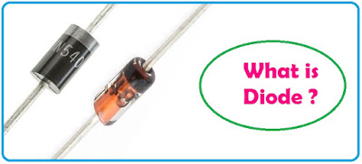
what is diode?


here present the diode in this article you can get knowledge about diode.

Image result for what is diode
Defination: A diode is a two-terminal component in electronics with a unidirectional flow of current. It offers low resistance in the direction of current flow and offers high resistance in the opposite direction. Diodes are mostly used to prevent damage to components, especially due to electromotive force in circuits which are usually polarized.
•A diode is a 2 lead semiconductor that acts as a one way gate to electron flow. – Diode allows current to pass in only one direction.
•A pn-junction diode is formed by joining together n-type and p-type silicon.
•In practice, as the n-type Si crystal is being grown, the process is abruptly altered to grow p-type Si crystal. Finally, a glass or plastic coating is placed around the joined crystal.
•The p-side is called anode and the n-side is called cathode.
 •When the anode and cathode of a pn-junction diode are connected to external voltage such that the potential at anode is higher than the potential at cathode, the diode is said to be forward biased.
–In a forward-biased diode current is allowed to flow through the device.
•When potential at anode is smaller than the potential at cathode, the diode is said to be reverse biased. In a reverse-biased diode current is blocked.
Image result for what is diode
how is the work of diode :

forword biased:
• When a diode is connected to a battery as shown, electrons from the n-side and holes from the p-side are forced toward the center by the electrical field supplied by the battery. The electrons and holes combine causing the current to pass through the diode. When a diode is arranged in this way, it is said to be forward biased.


• A diode’s one-way gate feature does not work all the time.
 • Typically for silicon diodes, an applied voltage of 0.6V or greater is needed, otherwise, the diode will not conduct.
 • This feature is useful in forming a voltage-sensitive switch. 
• I-V characteristics for silicon and germanium diodes is shown below.


reversed biased:
• When a diode is connected to a battery as shown, holes in the nside are forced to the left while electrons in the p-side are forced to the right. This results in an empty zone around the pn- junction that is free of charge carries creating a depletion region. This depletion region acts as a insulator preventing current from flowing through the diode. When a diode is arranged in this way, it is said to be reverse biased.


wide renge of applications are used :
  • Rectifiers
  • Switches
  • Signal modulators
  • Oscillators
  • Signal mixers
  • Signal limiters
  • Voltage regulators.

inverter

here present the inverter. in this artical you can get Knowledge about of inverter.applications of the inverter. single bridge inverter.  full bridge inverter Characteristics of a inverter.


We
Image result for inverter

•An inverter is an electrical circuit capable of turning dcpower into AC power, while at the same time regulating the voltage, current, and frequency of the signal.

• An inverter is a device that changes or inverts direct current (DC) input to alternating current (AC) output.

•It doesn't "create" or "make" electricity, just changes it from one form to another. DC in is changed to AC out.

• Output is usually 120 or 240 volts at depending on the country. 

•Inverters are often a good choice for   applications that require the main engine to operate at a job site. i.e. powering hydraulic systems or air compressors.

• Since, inverters are electronic devices, we   don't have the noise from a separate engine.

•  An inverter requires no fuel and virtually no maintenance.
                         
•  Since, inverter output is fully voltage and  frequency regulated and functions independently from the speed of the engine.

•Inverters come in all different shapes and sizes, for all different purposes.

•Inverters vary in output from 50 – 5,000 W.

application:


1    DC Power source utilization   
2    Uninterruptible power supplies
3    Induction heating
4   HVDC power transmission
5   Variable-frequency drives
6   Electric vehicle drives  
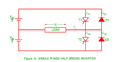
single phase half bridge inverter:
Image result for 1 phase half bridgeinverter
waveform:
Related image

single phase full bridge inverter:


waveform: