8085 pin functions
8085 pin functions.

the 8085 pin configuration and functional pin diagram of 8085 respectivly.
the signals of 8085 can be classified in to seven groups according to their functions.
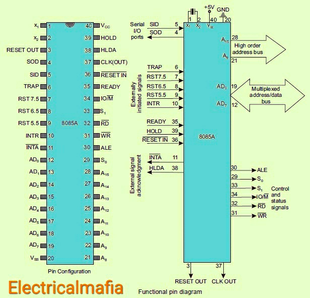
8085 pin functions


1. power supply and frequency signals.
2. data bus and address bus.
3. contol bus.
4. interrupt signals.
5. serial input output signals.
6. DMA signals.
7. reset signals.

1.  Power Supply and Frequency Signals

i)Vcc: it requires a single+5 V power supply.

ii)Vss:  ground reference.

iii)X1 and X2(Input):
A tuned circuit like LC, RC or crystal is connected at theset two pins.The internal clock generator divides oscillator frequency by 2,therefore, to operate a system at 3 MHz, the crystal of the tuned circuit must have a frequency of 6 MHz.

iv)CLK OUT(Output):
This signal is used as a system clock for other devices.Its  frequency is half the oscillator frequency.

2. Data Bus and Address Bus

A)ADo to AD7(Input/Output):
The 8-bit data bus(D0-D7)is multiplexed with a lower half(A0-A7)of the 16-bit address bus. During first part of the machine cycle
(T1), smaller 8 bits of memory address or I/O address appear on the bus. During remaining part of the machine cycle(T2  and T3) these lines are used as a bi-directional data bus.

B)A7 to A15(Output): 
Thus The upper half of the 16-bit address appears on the address lines.
This lines are exclusively used for the most significant of the 16-bit address lines.

3 Control and Status Signals

A)ALE(Address Latch Enable)(Output):
We know that the AD0 to AD7 lines are multiplexed and lower half of the address(A0-A7)is available only during T1, of the machine cycle.These lower half of address is also necessary during T2 and T3 of machine cycle to access specific location in memory or I/O port.This means that the lower half of the address be latched in T1 of the machine cycle, so that it is available throughout the machine cycle.The latching of lower half of the address bus is done by using external latch and ALE signal from 8085.

B)RD  and WR (Output):
The low on RD indicates that the data must be read from the selected memory location or Input output port via data bus. the low on WR indicates that the data must be written into the selected memory location or I/O port via data bus.

C)IO/M, S0 and S1(Output):
IO/M indicates whether I/O operation or memory operation it is  carried out. S1 and S0 indicate that the type of machine cycle in progress.

D)READY(Input):
It is used by the microprocessor to sense whether a peripheral is ready or not for data transfer.,If not,  the processor waits. It is  used to synchronize slower peripherals to the microprocessor.

4 Interrupt Signals

Hardware Interrupts (Input):
The 8085 have a five hardware interrupt signals: RST 5.5, RST 6.5 ,RST 7.5, TRAP and INTR. The microprocessor recognizes interrupt requests on this lines at the end of the current instruction execution.

INTA(Output):
The INTA(Interrupt Acknowledge) signal is used to indicate that the processor has acknowledged an INTR interrupt.

5 Serial I/O Signals

A)SID (Serial I/P Data)(input):
This input signal is used to accept serial data  bit from the external device.

B)SOD(Serial O/P Data)(Output):
These is an output signal which enables the
transmission of the  serial data bit by bit to the external device.

6.  DMA signal

A)HOLD(Input):
This signal is indicate that  the another master is requesting for the use of address bus,data bus and control bus.

B)HLDA(Output):
Thus the active high signal is used to acknowledge HOLD request.

7. Reset Signals

A)RESET IN(Input):A low on this pin
1)Sets the program counter to zero(0000H)and clears the INTE fiag.
2)Resets the interrupt enable and HLDA flip-flops.
3)Tri-states the data bus,address bus and control bus.
(Note:Only during RESET is active).
4)Affects the contents of processor's internal registers randomly.

B)RESET OUT(Output):This active high signal indicates that processor is being
reset.These signal is synchronized to the processor clock and it can be used to reset other devices connected in the system.
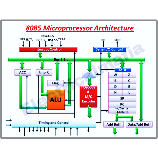
Architecture of 8085 microprocessor

Architecture of 8085 microprocessor

architecture of 8085microprocessor
8085 microprocessor architecture
(A)Register structure:


architecture of 8085microprocessor
Register structure
The shaded portion of this register model is called programmer's model of 8085.
 It includes six 8-bit registers -(B,C,D,E,H and L) one accumulator, one flag register and two 16-bit registers(SP and PC).All these registers are accessible to programmer and hence they are included in the programmer's model. The remaining registers-Temporary,W and z are note accessible to the Programmers;they are used by microprocessor for internal,intermediate operations.

Use of W and Z registers

 That is a CALL instruction is used to transfer program control to a subprogram or subroutine.This instruction pushes the current PC contents onto the stack and loads the given address into the program counter.The  address is temporarily stored in the W and Z registers and placed on,the bus for the fetch cycle. the program control is transferred to the address given in the instructional. XCHG instruction  exchanges the contents of H with D and L with E. At this time of exchange W and Z registers are used for temporary storage of data.

1.General purpose registers:

 B,C,D,E,H and L are 8-bit general purpose registers can be used as a separate 8-bit registers or as 16-bit register pairs,BC,DE and HL. HL pair is  also functions as a  memory pointer. or data pointer

2.Special purpose registers:

2.1) Register A(Accumulator): It is a tri-state eight bit register.It is extensively used in arithmetic,logic,load and store operations, as well'as in,input/output(I/0) operations.the result of arithmetic and logical operations is stored in register A. Hence it is also identified as accumulator.

2.2) Flag Register(Program status word): It is an 8-bit register,in which five of the bits carry significant information in the form of flags: S(Sign flag), Z(Zero flag), AC (Auxiliary Carry flag), P(Parity flag),and CY(Carry flag)

D7D6D5D4D3D2D1D0
SZACPCY
S-Sign flag:  After the execution of arithmetic or logical operations,if bit Dz of the result is 1,the sign flag is set.In a given byte if D-is 1,the number will be viewed as negative number.If D-is O,the number will be considered as positive number.

Z-Zero flag: This flag is sets if the result of operation in ALU is zero and the flag is resets if result is non zero.The zero flag is also set if an certain the register content becomes zero following  increment or decrement operation of the register. 

AC-Auxiliary Carry flag:This is set if there is overflow out of bit 3 i.e., carry from lower nibble to higher nibble(D3 bit to D4bit). This AC flag is used for BCD Operations and it is not available for the programmer.

P-Parity flag: Parity is defined by the number of ones present in the accumulator. Atter an arithmetic or logical operation if the result has an even number of ones, l.e.even parity,the flag is set.If the parity is odd,flag is reset.

CY-Carry flag:This flag is set if there is an overflow out of bit 7.The carry flag is  that the serves as a borrow flag for subtraction.In both the examples shown below,the carry flag is set.
    
2.3) Instruction register: In a typical processor operation,the processor first fetches the opcode of instruction from memory (i.e. it  places an address on the address bus and memory responds by placing the data stored at the specified address on the data bus). CPU stores this opcode in a register called the instruction register.This opcode is further sent to the instruction decoder to select one of the 256 alternatives.

2.4) Program Counter(PC): the Program is a sequence of instructions. As it is mentioned earlier,microprocessor fetches these instructions from the memory and executes them sequentially.The program counter is a special purpose register,which,at a given time, stores the address of the next instruction to be fetched.Since address of 8085 is 16-bit, the PC is 16-bit.Program Counter acts as a pointer to the next instruction.How processor increments program counter depends on the nature of the instruction;for one byte instruction it increments program counter by one, for two byte instruction it is  increments program counter by two and  three byte instruction it is increments program counter by three such that program counter always points to the address of the next instruction.

2.5)Stack Pointer(SP): This  stack is a reserved area of the memory in the RAM where temporary information may be stored.A 16-bit stack pointer is used to hold the address of the most recent stack entry.

(B) Arithmetic Logic Unit(ALU)

The 8085's ALU performs arithmetic and logical functions on eight bit variables.The arithmetic unit performs bitwise fundamental arithmetic operations such as addition and subtraction.The logic unit performs logical operations such as complement, AND,OR and EX-OR, as well as and clear and rotate. The ALU also looks after the branching decisions.

(C) Instruction Decoder and Machine Cycle Encoder

The instruction decoder decodes the opcode and accordingly gives information to the timing and control circuit.
The microprocessor executes a seven different types of machine cycles.If a gives the information about which machine cycle is currently executing in the encoded form on the S0 S1,and IO/M lines.This task is done by machine cycle encoder.

(D) Address Buffer

That  is a 8-bit unidirectional tristate buffer.It is used to drive external high order address bus(A15 -A8).

(E) Address/Data Buffer

This is an 8-bit bi-directional buffer.It is used to drive multiplexed address/data bus, i.e.low order address bus(A7-Ao) and data bus(D7-Do).

(F) Incrementer/Decrementer Address Latch:

This is a 16-bit register is used to increment or decrement the contents of program counter or stack pointer.

(G) Interrupt Control

That is the interrupt control block has five interrupt inputs RST 5.5, RST 6.5, RST 7.5, TRAP and INTR and one acknowledge signal INTA. It controls the interrupt activity of 8085 microprocessor.

(H) Serial I/O Control

The  8085 microprocessors serial I/O control provides two lines,SOD and SID for serial communication.The Serial Output Data(SOD)line is used to send data serially and Serial Input Data(SID)line is used to receive data serially.

(I) Timing and Control Circuitry

The control circuitry in the processor of 8085 microprocessor is responsible for all the operations.The control circuitry and hence the operations in 8085 are synchronized with the help of clock signal. Along with the control of fetching and decoding operations and generating appropriate signals for instruction execution,control circuitry also generates signals required to interface external devices to the processor of 8085.

(J) Instruction Execution and Data Flow in 8085

In order to execute program,the starting address of the program is loaded into the Program Counter(PC).
The 8085 sends the contents of PC as an address on the address bus and activates RD control signal.
Upon receiving the address and RD signal memory puts the contents of addressed memory location on the data bus which is an opcode of an instruction.
Meanwhile,PC is incremented to point the next memory location in the program sequence.
RD signal is deactivated and opcode is loaded into the instruction register via internal bus of microprocessor. 
The instruction decoding unit decodes the instruction and provides information to the timing and control unit to generate necessary signals for instruction execution.

Types of memories in microprocessor system

Here present the article about the types of memories in microprocessor system.

  • There are two basic kinds of memory used in microprocessor systems - memories are classified as two types volatile memories and non- volatile memories.
  • Volatile memories is random access memory(RAM) and non-volatile memories is read only memory(ROM).
  • It is a volatile memory as a retain their stat as long as power is applied or data loses when the power is turned off.
  • Other hand non- volatile momory can hold data even if power is turned off.

⏩Random access memory(RAM):

  • The memory in which the time taken to transfer information to or from any desired random location is always the same is called random access memory.
  • There are two types of RAMs
  1. Static RAM
  2. Dynamic RAM

1. Static RAM

  • Memories that consists of circuits capable of retaining their state as long as power is applied are know as static RAM memories.
  • These are random access memory (RAM) and hence combinely called static RAM memories.

Advantages of SRAM:

  1.  Fast memory (less access time) 
  2.  Refreshing circuit is not required.

Disadvantages of SRAM: 

  1. Low package density 
  2.  Costly

2. Dynamic RAM

  • Dynamic RAM stores the data as a charge on the capacitor and they refreshing of charge on the capacitor after every few milliseconds to hold the data even if power is ON.

Advantages of DRAM: 

  1. High package density 
  2. Low cost

Disadvantages of DRAM: 

  1.  Required refreshing circuit to maintain or refresh charge on the capacitor, every after few milliseconds.

Comparison between SRAM and DRAM


⏩Read only memory(ROM):

  • It is the memory that performs the read only operation. 
  • We can't write data in read only memories.
  • It is non - volatile memory. 
  • Generally ROM is used to store the binery codes for the sequence of instructions you want the computer to carry out and data such as look up tables. This is because this type of information does not change.
  • There are four types of ROM :
  1. Masked ROM 
  2. PROM
  3. EPROM
  4. EEPROM

1. masked ROM:

  • the program or data are permanently installed at the time of manufacturing as per requirement.
  •  The data cannot be altered. 
  • The process of permanent recording is expensive but economic for large quantities.

2. PROM(Programmable Read Only Memory)

  • PROM Is Programmable Read Only Memory.
  • This memory has nichrome or polysilicon wires arrenged in a matrix these wires can be functionally viewed as diode or fuses.
  • This memory can be programmed by user with a special PROM programmer that selectively burns the fuses according to the bit pattern to be stored the process is known as burning the PROM.

3. EPROM(Erasable programmable read only memory)

  • The memory stores a bit by charging the floating gate of an FET.
  • Information is stored by using an EPROM programmer.
  • Which applies high voltage to charge the gate. 
  • All the information can be erased by exposing the chip to ultraviolet light through its quarts window and the chip can be reprogrammed because the chip can be reused many times.
  • This memory is ideally sulted for product development experiment projects and collage laboratories.
  • The disadvantage of EPROM are 
  1. It must be taken out of the circuit to erase
  2. The entire chip must be erased 
  3. The erasing process takes is to 20 minutes.

4. EEPROM(Electrically Erasable programmable read only memory)

  • This memory is functionally simillar to EPROM except than that information can be altered by using electrical signals at the register level rather than erasing all the information.
  • This has on advantage in field and remote control application. 
  • In microprocessor system software update is a common occurence if EEPROM are used in the system.
  • They can be updated from a central computer by using a remote link via telephone lines.
  • This memory includes a chip Erase mode where by the entire chip can be earased in 10 minutes vs 1 sec. To 20 min. To earase an EPROM however this memory is expensive compared to EPROM or flash memory.